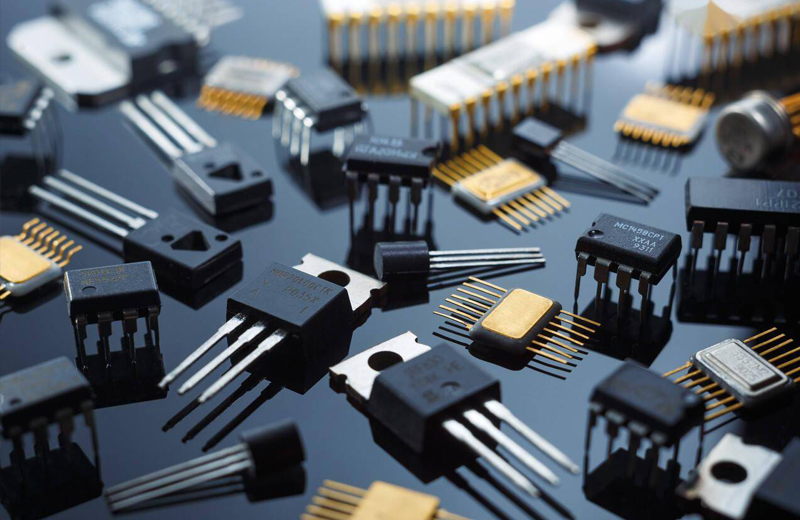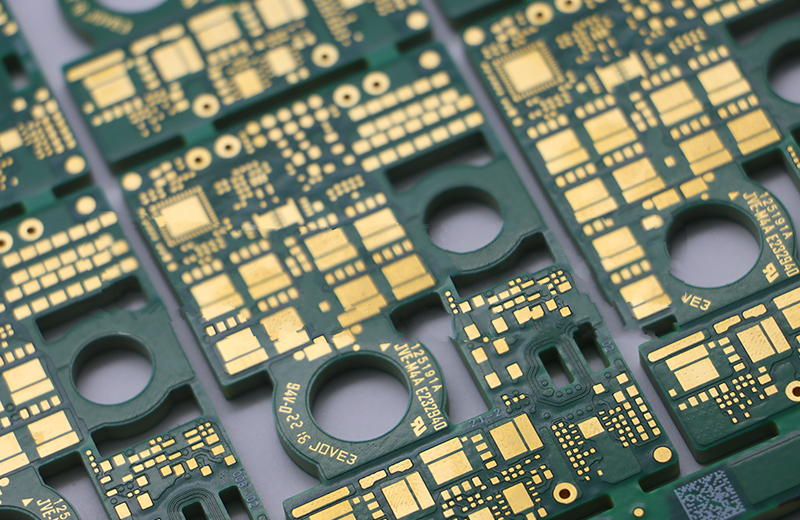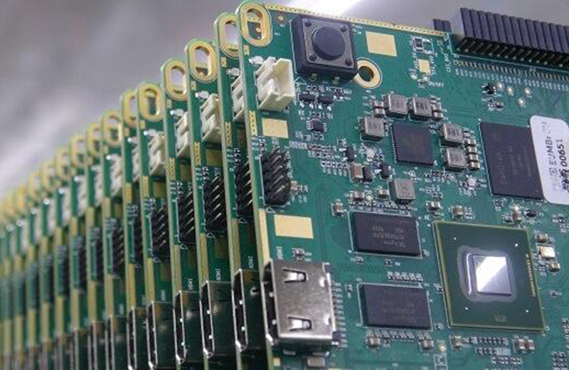

In the field of PCB (printed circuit board) manufacturing, gold finger design is widely used in electronic devices such as memory modules, graphics cards, network interface cards, etc. due to its critical role in high reliability data transmission. The design and manufacturing of the gold finger board require extremely high precision and strict process control. Any small mistake may lead to the failure of the finished product, thereby increasing costs and affecting product performance.
This article will conduct an in-depth analysis of a practical case - the problem of exposed copper on the inner layer of the gold finger board at the beveled edge, and explore its causes and corresponding improvement measures.
1、 Case background
Recently, a quality issue occurred on a PCB production line due to a mismatch between the design and manufacturing process of the gold finger board. Specifically, during the oblique edge processing, it was found that some of the inner copper sheets of the gold finger boards were exposed in the oblique edge area, which directly led to the scrapping of this batch of boards and had a serious impact on production efficiency and cost.
2、 Cause analysis
1. Negligence in film design: The core of the problem lies in the insufficient consideration of the special characteristics of the gold finger board during the design phase of the film (i.e. photo negative film used for circuit graphic transfer). Gold finger boards usually require beveled edge treatment to ensure good insertion and electrical contact performance, but the parameters of the beveled edge process were not taken into consideration during the design of this batch, resulting in the layout of the inner copper sheet not being able to reasonably avoid the beveled edge area.
2. Poor communication in the process flow: During the transition from design to manufacturing, there is insufficient communication regarding the special requirements of specific board types (such as metal finger boards), which leads to the manufacturing department producing without fully understanding the design intent. This is also an important reason for the occurrence of problems.
3、 Improvement measures
To avoid such problems from happening again, the following targeted improvement measures need to be taken:
1. Comprehensive review before film production
-Face to face review of MI (Manufacturing Instruction Document): Before making the film, the process engineer must carefully read and understand every item of MI to ensure a comprehensive grasp of the basic information such as the type, size, number of layers, and special process requirements of the board. Especially for the gold finger board, special attention should be paid to its unique beveled edge processing requirements.
2. Design rule adjustment
-Application of Inner Copper Skin Avoidance Calculation Formula: Based on the provided formula 'A=(Upper Limit of Diagonal Edge -1st and 2nd Thickness/tga)+(10-20 MIL)', where 'a' is the angle of the hypotenuse, the avoidance distance of the inner copper skin in the hypotenuse area can be accurately calculated. This requires designers to incorporate this calculation into the PCB layout at the early stage of design, ensuring sufficient safety distance between the inner copper skin and the beveled edge to avoid copper exposure during subsequent processing.
3. Strengthen cross departmental communication
-Establish a specialized communication mechanism: set up dedicated project meetings or use digital tools to ensure accurate and error free transmission of information regarding special process requirements between design, engineering, production, and quality control departments. For high demand products such as gold finger boards, special emphasis should be placed on their process characteristics to ensure that personnel at all stages have a clear understanding of them.
4、 Process validation and training
-Implement process validation: After a new or modified design, conduct small-scale trial production and strict inspection to ensure that all process steps, including beveled edge treatment, meet the design requirements.
-Employee training: Regularly provide special process training for production line employees, especially for the processing details of the gold finger board, to improve employees' awareness of process sensitivity and ensure that everyone can operate according to the optimized process.
By implementing the above measures, it is possible to effectively prevent the problem of exposed copper in the inner layer of the gold finger board during production, improve product quality and production efficiency, and reduce defect rates and production costs. In the highly competitive electronic manufacturing industry, details determine success or failure, so fine management of every link is particularly important.